Hardware Setup
Required Hardware
ADRV9361 Module
The 802.11 FPGA Design targets the ADI ADRV9361 module. This board integrates the Zynq 7Z035 processor, AD9361 radio, and various peripherals. This module requires a carrier board.
ADI makes a second ADRV9361 module (ADI ADRV9364) with a smaller Zynq device and single-antenna radio transceiver (AD9364). The current 802.11 FPGA Design does not support the ADRV9364 module.
ADRV9361 Carrier
The 802.11 FPGA Design targets the ADRV9361 FMC carrier board (ADI ADRV1CRR-FMC). The ADRV9361 module mounts on this carrier board. The carrier provides various peripheral interfaces and an FMC slot.
The ETHERNET1 interface is used as the bridged interface for Ethernet Rx processing. The ETHERNET2 interface is used for wlan_exp command processing.
ADI makes a smaller Breakout ADRV9361 carrier (ADI ADRV1CRR-BOB). The current 802.11 FPGA Design does not support the Breakout Carrier.
Hardware Configuration
The 802.11 design requires specific configuration of the ADRV9361 hardware.
Boot Mode
The ADRV9361 module uses 3 switches to configure the Zynq boot mode. The ADRV9361 boot mode switches are labeled S1, S3 and S4. The figure below illustrates the switch locations. Each switch has a white dot indicating the “Off” position.
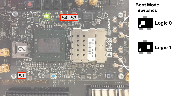
Fig. 2.4 ADRV9361 boot mode switch locations
The table below gives the switch settings for each boot mode. This user guide assumes the Zynq is configured for FMC Carrier SD Boot.
| Boot Mode | S1 | S3 | S4 |
|---|---|---|---|
| Cascade JTAG | 0 | 0 | x |
| QSPI | 1 | 0 | x |
| MicroSD Card (SOM) | 1 | 1 | 0 |
| SD Card (FMC carrier) | 1 | 1 | 1 |
The Zynq device can be configured via JTAG in any boot mode. We recommend leaving S1/S3/S4 set to 1 (selecting FMC carrier SD boot).
FMC Module Configuration
The 802.11 FPGA design supports the Xilinx XM105 FMC module by default (see below). The XM105 module is not required. Using the FPGA design with other FMC modules requires modifying the FPGA design.
When using the XM105 a 2-pin shunt must be connected between the TDI and TDO pins. This shunt completes the JTAG chain when the module is mounted on the ADRV9361 FMC carrier. When using other FMC modules refer to the module documentation for how to use JTAG.
The ADRV9361 FMC carrier has a 3-pin jumper which sets the voltage of the VADJ rail. This jumper must be set properly before mounting an FMC module. When using the Xilinx XM105 debug module (see below) VADJ can be set to any voltage. When using other FMC modules, refer to the module documentation for its VADJ setting.
Additional Resources
Analog Devices maintains documentation for the ADRV9361 platform on their wiki. The ADI wiki also contains documentation for the ADI cores and code for the AD9361 transceiver interface.
The Analog Devices ADRV9361 platform was previously known as PicoZed SDR. The PicoZed SDR hardware was developed jointly by ADI and Avnet. ADI re-branded the platform when the ADI/Avnet relationship ended in 2017.
The original Avnet PicoZed SDR documentation is still available and remains a useful resource for using the ADRV9361 hardware.
Required Accessories
JTAG Cable
The Vivado SDK and debug tools require a JTAG connection between the PC and FPGA board. Any JTAG cable supported by Vivado will work with the 802.11 design. We recommend the Digilent JTAG-HS3 cable. The JTAG cable must be connected to the 14-pin JTAG header on the ADRV9361 FMC carrier (labeled P15 JTAG).
RF accessories
The ADRV9361 uses U.FL jacks for its RF connections and includes U.FL - SMA plug adapter cables. You must supply the additional RF accessories required for your application. For example to test multiple nodes over a wired connection, you will need RF cables with SMA jacks, attenuators, splitters/combiners, etc. None of the antennas included with the ADRV9361 hardware cover the 2.4GHz band.
Recommended Hardware
The 802.11 FPGA Design supports additional hardware which may be useful in some experiments.
ADI PA/LNA Module
The ADI ADRV9361 FMC Carrier has a slot for an “RF Personality Module”, intended to implement front-end filters and amplifiers for specific applications.
ADI has released one RF Personality Module, the ADI ADPZSDR2400TDD-EB. This module implements filters, Rx LNA, and Tx PA for the 2.4 GHz band.
The 802.11 design supports this PA/LNA module. The module will be automatically detected at boot. The MAC C code will adjust required parameters (Tx power range, Rx power mapping, etc.) automatically when the module is installed. The front-end module detection status is printed to the CPU Low UART at boot.
USB-UART PMOD Module
Refer to the ADRV9361 UART page for details.
XM105 Debug FMC Module
The ADI ADRV9361 FMC carrier provides an FMC slot connected to Zynq PL IO pins. The 802.11 FPGA Design supports the Xilinx XM105 debug module. The 802.11 design routes various status signals to the XM105 headers to observe MAC/PHY timing on an oscilloscope. The design also uses the 4 green LEDs on the XM105 module for additional activity indicators.
SMA Bracket
When the ADRV9361 module is used without a RF personality module, external RF cables are connected directly to the fragile U.FL jacks. This connection makes it easy to damage the ADRV9361 hardware.
Another ADRV9361 platform user designed a plastic bracket which mounts to the FMC carrier and provides a bulkhead for the U.FL - SMA adapter cables.
The bracket was originally advertised on the PicoZed SDR Forums: http://zedboard.org/content/sma-bracket-fmc-carrier
Unfortunately the source post is no longer available. We previously submitted the 3D model to Sculpteo to print brackets for our kits. The results were great. It should be possible to re-order the same job from Sculpteo at https://www.sculpteo.com/en/print/pzsdr2-l-bracket-v1-12/Dsemznme.