5. FPGA Design
The Mango 802.11 FPGA Design is built in Xilinx Vivado. The entire 802.11 FPGA design is implemented as an IP Integrator (IPI) block diagram. The IPI block diagram defines the complete logic design for the PL (Programmable Logic) section of the Xilinx device. The FPGA design makes extensive use of the PL/PS interfaces to connect the logic design to software running in the ARM CPUs. The FPGA design implements the MAC and PHY cores, radio interfaces, and off-chip peripheral controllers.
- For more details on individual IP cores, refer to:
Mango provides reference IPI designs for supported hardware platforms. For details on using these reference designs in Vivado refer to the Vivado project usage guide.
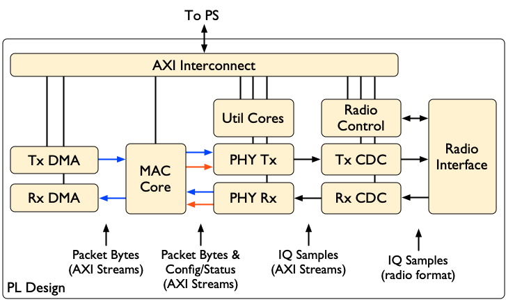
Fig. 5.1 FPGA Design block diagram